Pioneering 110 GHz 8-Inch Wafer-Level TGV Interposer for Next-Gen Optoelectronics
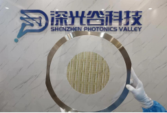
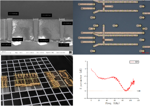
Shenzhen Photonics Valley Technology Co., Ltd. (SPVTECH), in collaboration with Shanghai Jiaotong University and Shenzhen University, has successfully developed China’s first 8-inch wafer-level Through Glass Via (TGV) optoelectronic interposer process, achieving a measured bandwidth of 110 GHz. This wafer-level TGV interposer supports 2.5D and 3D optoelectronic integrated packaging, offering high-speed, high-density, high-reliability, and cost-effective co-packaged optics (CPO) solutions for VCSEL, DML, EML, silicon photonics, and lithium niobate modules. Leveraging laser-induced deep etching and multi-layer redistribution (RDL) technology, SPVTECH’s process attains a through-glass aspect ratio of 4:1 with substrate thickness of 230 μm and surface flatness of 1.2 μm.
Breakthrough Details
Wafer-Level Process and Performance
First Domestic 8-Inch Implementation
SPVTECH realized wafer-level fabrication of TGV interposers on 8-inch glass substrates, marking a significant milestone in domestic optoelectronic packaging capabilities.Laser-Induced Deep Etching & RDL Integration
The interposer is produced via femtosecond laser-induced deep etching (LIDE) combined with multi-layer redistribution layers, enabling a through-hole aspect ratio of 4:1 and trench depths of 60 μm.High-Frequency Performance
Both the metallized through-glass vias and RDL traces exhibit bandwidth exceeding 110 GHz, validated through experimental and simulation methods facing 128-GBaud 2.5D CPO test signals.
Packaging and Integration Capabilities
RDL Layers & Flip-Chip Support
Supports 2 + 1 RDL layers, enabling flip-chip assembly of both electrical driver chips and optical chips (EML, SOA, silicon photonics, lithium niobate).Optical Fiber Array Alignment
The interposer design accommodates precise coupling alignment for fiber-array packages, facilitating co-packaged optics (CPO) integration in data-center and AI-compute modules.
Applications and Future Outlook
Glass-based packaging technologies, such as TGV interposers, have garnered attention for advanced passive devices, microdisplays, AR/VR, and CPO scenarios due to glass’s favorable optical transparency and reliability. On September 18, 2023, Intel unveiled its most advanced processor using a glass substrate, with mass production slated between 2026 and 2030—underscoring the disruptive potential of glass-based CPO for data centers and AI accelerators.
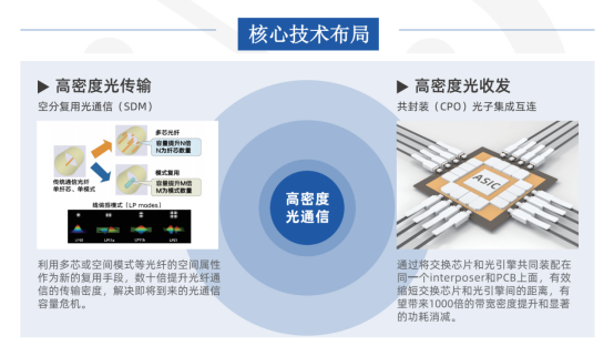
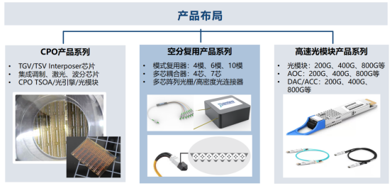
SPVTECH plans to integrate its TGV interposer with high-density space-division multiplexing (SDM) and laser-direct-writing optical connectors, forming end-to-end glass-in-laser-written connection solutions. These efforts aim to enhance link density and support applications spanning data centers, computing clusters, and high-capacity optical transmission networks.

